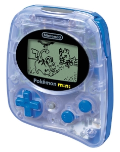
Difference between revisions of "Pokemon Mini"
From SublabWiki
(→Pokemon Mini Hardware Overview) |
(→Pokemon Mini Hardware Overview) |
||
| Line 3: | Line 3: | ||
The Pokemon Mini is a hand held created by Nintendo R&D3 around 1999. The hardware as engineered entirely in-house and does not appear to contain any off the shelf parts other than a few slightly less important crucial elements like the LCD controller and internal EEPROM. The system is built around a 4mhz custom CPU (with a 4 cycle data access period), with a 4k bios image, 4k of ram and a 21-bit cartridge bus. The internal memory map is decoded as 24-bit with no known mirrors. The entire system is controlled by writting to 256 hardware registers, most of which are [[Open-Bus]]. | The Pokemon Mini is a hand held created by Nintendo R&D3 around 1999. The hardware as engineered entirely in-house and does not appear to contain any off the shelf parts other than a few slightly less important crucial elements like the LCD controller and internal EEPROM. The system is built around a 4mhz custom CPU (with a 4 cycle data access period), with a 4k bios image, 4k of ram and a 21-bit cartridge bus. The internal memory map is decoded as 24-bit with no known mirrors. The entire system is controlled by writting to 256 hardware registers, most of which are [[Open-Bus]]. | ||
| − | * [[ | + | * [[S1C88_Core|The Pokemon Mini CPU: S1C88]] |
| − | ** [[ | + | ** [[S1C88_Core|S1C88 Overview]] |
** [[PM_InstructionList|Instruction Set]] | ** [[PM_InstructionList|Instruction Set]] | ||
** [[PM_IRQs|Interrupt Hardware]] | ** [[PM_IRQs|Interrupt Hardware]] | ||
Revision as of 22:15, 10 July 2015
Pokemon Mini Hardware Overview
The Pokemon Mini is a hand held created by Nintendo R&D3 around 1999. The hardware as engineered entirely in-house and does not appear to contain any off the shelf parts other than a few slightly less important crucial elements like the LCD controller and internal EEPROM. The system is built around a 4mhz custom CPU (with a 4 cycle data access period), with a 4k bios image, 4k of ram and a 21-bit cartridge bus. The internal memory map is decoded as 24-bit with no known mirrors. The entire system is controlled by writting to 256 hardware registers, most of which are Open-Bus.
- The Pokemon Mini CPU: S1C88
- The Memory Map
- Internal BIOS
- The Memory
- The Hardware Registers
- Cartridge Memory
